The Types of Semiconductor Reliability and Quality Testing

In this guide, we’re going to explore the different types of tests needed to qualify semiconductor devices, and which tests are useful for product characterization and quality assurance as those products leave the production line.

We’ll take you through the testing requirements at each step of the product lifecycle and make sure you understand:

  • The definition of each test
  • Why testing is done at this stage
  • The key objectives of each test
  • The factors for successful testing
  • And test equipment requirements


There are three main categories of test types:

1

Intrinsic reliability testing

2

Application testing

3

Quality assurance or extrinsic reliability testing

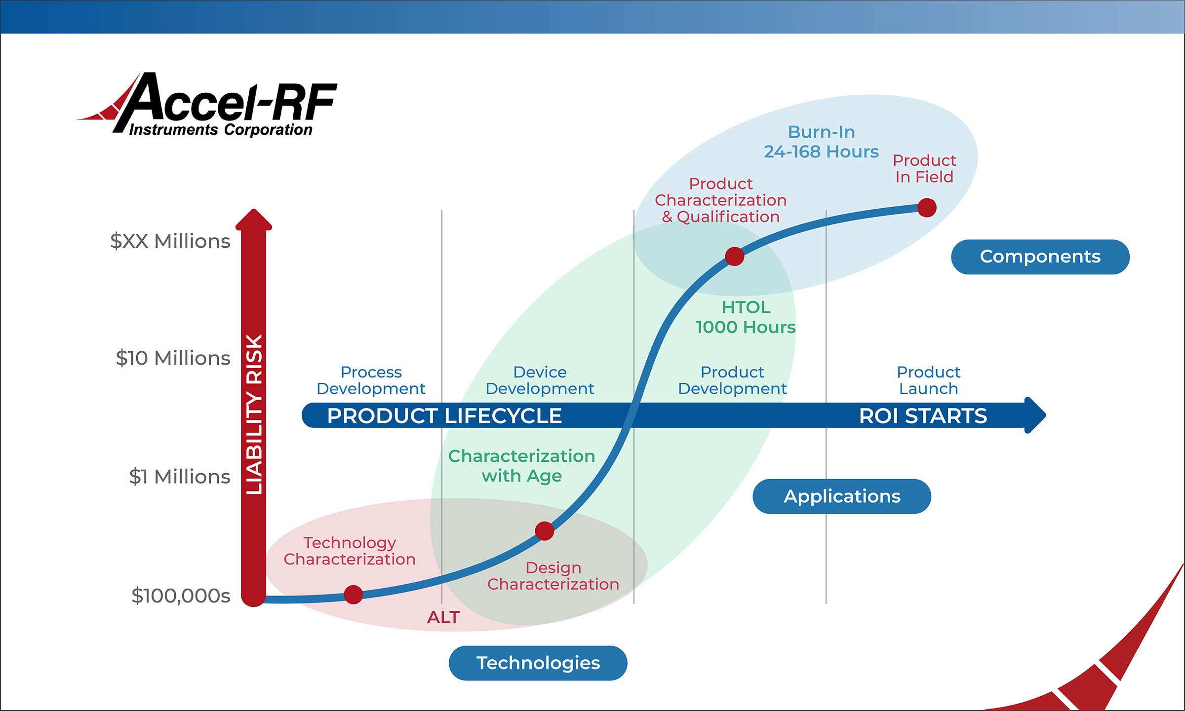
It’s helpful to view these tests in the context of the product development lifecycle. The tests performed early in the process development phase have different requirements and objectives than those performed on finished devices heading into the market. As the product development lifecycle charges ahead, the investment risk of a failure increases at pace. So it’s critical to understand how to leverage each test type to maximize your return on investment.

Testing for Intrinsic Reliability

Learning to work with new materials in a manufacturing setting is a process that requires some time. In addition, different characteristics inherent to a material’s molecular structure create unfamiliar operational and environmental constraints. For example, producing wafered semiconductor layers ready for packaging is entirely different when working with a GaN substrate rather than one made from Silicon.

Intrinsic reliability testing allows test experts to learn how to overcome inherent performance and failure issues, tweak production recipes to mitigate defects created by the process, and then fully exploit the beneficial characteristics of the new material.

Reliability shortcomings from design to production can be minimized by incorporating, as early in the development cycle as possible, statistical process control methodologies in the fabrication of the part and by performing life testing measurements. Implementing these techniques forces reliability growth to occur in conjunction with product development. For the manufacturer, this means a quicker time-to-market cycle of a reliable product that will not require costly warranty repair or replacement. For the user, it means that the state-of-the-art product can be confidently incorporated into their advanced system without the additional cost and delivery time increase associated with a traditional, highly reliable part procurement.

What is Accelerated Life Testing?

Since most semiconductor applications require device lifetimes of many years, a practical approach to acquiring reliability data in a reasonable amount of time is to employ highly accelerated life testing. ALT is designed to stress devices with RF, DC, and thermal stimuli to evaluate reliability and performance degradation. Running these tests at elevated temperatures makes it possible to reduce a component's failure time, thereby enabling data to be obtained in a shorter time than would otherwise be required to determine the operational lifetime of the device.

The Key Objectives of Accelerated Life Testing (ALT)

Since many high-power GaN parts need to last millions of hours in the field, one of the key components of generating meaningful reliability data is to perform ALT on a statistically significant number of devices for a period of time, typically 100s to 1000s of hours, until parametric failure, catastrophic failure, or another predefined condition occurs. Due to the nature of the Arrhenius equation and the effect of temperature acceleration, the life test data can be used to extrapolate the expected device lifetime.

Once the parts reach the failure criteria, they undergo failure analysis that informs changes to the device structure, e.g., metallization thickness or the way structures are etched and improvements to the fabrication process. 

Factors for Successful Accelerated Life Testing

Channel Temperature

Quantifying the channel temperature of a device is fundamental in obtaining accurate reliability predictions from accelerated temperature testing. A semiconductor transistor will have many areas where current flows and power dissipates during operation. Some of these active areas are far hotter than others. The chemical and physical changes that lead to failure occur in these hotter regions. Therefore, one needs to know the temperature of these regions to obtain accurate determinations of activation energy, a benchmark figure-of-merit for a chemical or mechanical process change in time.

The importance of accurately determining the channel temperature of each device submitted to a life test cannot be overstressed. Variables affecting the channel temperature include ambient temperature, device thermal resistance, package and mounting materials, power dissipation, and RF signal levels. The effects of channel temperature inaccuracies can skew attempts at obtaining accurate failure rate data from ALT processes involving RF devices.

ALT systems must have the capability to dynamically hold the channel temperature constant, typically ranging from 300°C to 400°C and higher, with varying DC and RF parametric changes during a long duration. This is very important to induce the desired physical change in the device in a controlled manner. Without this capability, the channel temperature, used as the acceleration parameter for determining failure times, would vary wildly during the test as power dissipation changes.

Fixturing

The key to achieving meaningful test data rests in the test fixture “chamber” that allows the part to operate with DC and RF signals applied and measured at extremely high temperatures. The fixture must have a large amount of thermal isolation between the device mounting area and other components used in the RF circuit design. The performance of key fixture components, such as the RF connectors, substrate material, and passive components used for impedance matching and stability, can shift with temperature.  Thermally isolating these elements from the extreme temperatures the Device Under Test (DUT) is subjected to will help maintain performance and prevent unwanted oscillations over the course of the test.

Multi-Channel Support

Statistics drive the accuracy of reliability testing, so the number of devices tested correlates directly with the mathematical meaningfulness of the test. Employing a test system with multiple channels provides the ability to analyze larger sets of devices instead of performing tests one device at a time. Multi-channel test systems offer manufacturers a distinct time advantage in quickly characterizing devices.

DC and RF Testing

Many companies can’t resist the temptation of substituting less complex and lower-cost DC testing when RF testing is required. A pernicious myth says that the testing results will be the same, so it’s a smart move. DC testing alone might produce some reasonably accurate lifetime prediction data, but that does not tell the whole story for manufacturers producing devices that process signals in the RF spectrum.

DC testing plays a vital role in verifying the intrinsic reliability characteristics of newly designed ICs. It costs less and is easier to implement because the additional RF source and measurement components are eliminated. Characterizing a semiconductor device, even devices designed to work in an RF application, with basic DC bias and swept DC parametrics is crucial for determining that the fabrication process and the resulting device structures are working as expected. DC bias tests can reveal fabrication defects and design characteristics that are out of performance tolerance in the semiconductor. DC cannot, however, take the place of RF testing to determine the suitability of an RF device for a given application. Manufacturers wishing to stay competitive in quickly changing markets must adopt a strategy that leverages both RF and DC testing to achieve complete results.

Maintaining a stable RF source over time is also a critical factor in RF ALT. Variation in the RF energy into and out of the device or drift in external temperature will have a detrimental effect on the test. Therefore, consistency in the RF supply and fixture to account for temperature changes to outside influence is vital to accurate test data.

Software and Analysis

An often overlooked component of ALT and reliability testing, generally, is having an integrated software tool that facilitates seamless data acquisition and analysis. Testing an array of devices under various stimulus conditions requires a robust and flexible hardware control system. The software must seamlessly configure the hardware for sophisticated biasing techniques, RF signal injection, and temperature control.

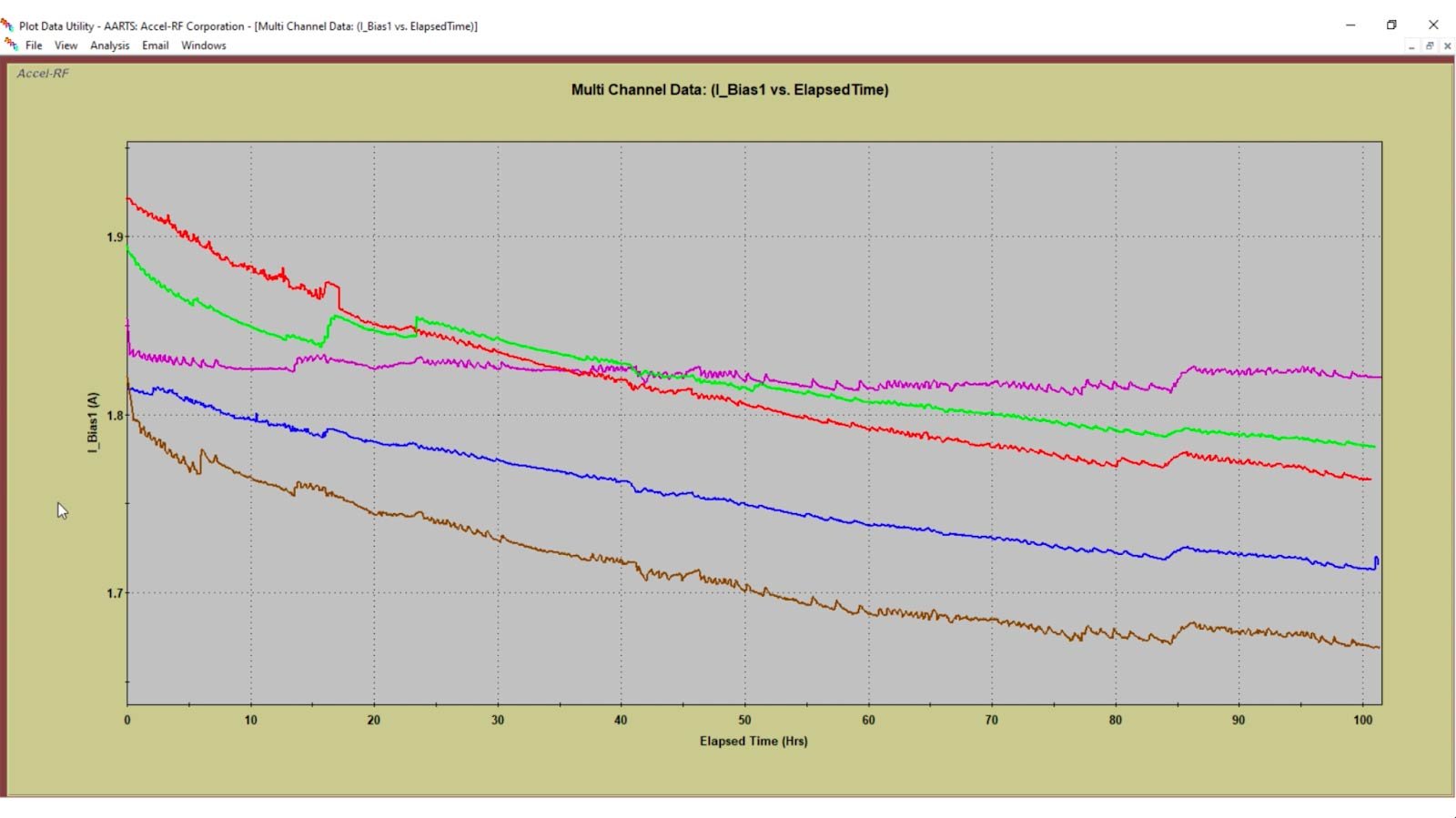
Once the equipment starts testing at the desired parameters, all of that rich data needs to be ingested by the software and extrapolated for value. Powerful data analytics are needed to prove device reliability by determining the mean time to failure and the distribution of a particular failure over time and temperature. Developing a software solution that easily obtains and presents the reliability data can be challenging.

LifeTest MultiChannel Data

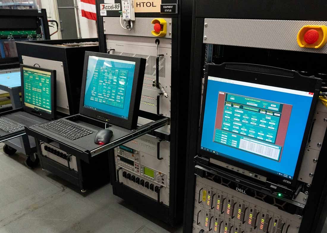
Accel-RF Accelerated Reliability Test Instruments

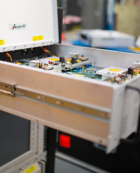
The expense of purchasing and maintaining the multiple pieces of test equipment needed to run all the required tests to meet multiple benchmarks adds up quickly. Companies that attempt in-house testing development typically struggle to keep up with the rapid pace of the changing and new uses for each device. A unique approach developed by Accel-RF is as elegant as it is economical: a modular design for device testing. This method allows companies to purchase one primary device testing unit and configure it as needed for different testing standards by adding more economical modules.

The Accel-RF Automated Accelerated Reliability Test Station (AARTS) systems are designed to stress devices with RF, DC, and thermal stimuli. The systems were also designed from inception to include RF stimulus – it was not added as an afterthought. This turnkey test system includes fully integrated software and hardware to control several independently controlled test positions.  Precise measurement and monitoring of test devices can be fully automated with the industry-standard LifeTest software.  Various frequency ranges (including mm-wave), power levels, and modulation types are supported.

Accel-RF systems feature multiple channels that can be individually configured at the fixture level to run specific analyses on each DUT. However, frequency parameters must be set in functional groups of eight. So a sixteen-channel system could test devices at two different frequencies simultaneously, one frequency setting for channels 1 - 8 and a second setting for channels 9 - 16. This capability gives chip makers attempting to enter various markets with a single device a significantly reduced time investment.

High-Temperature Reverse Bias (HTRB)

High-Temperature Reverse Bias is an industry-standard intrinsic reliability test that evaluates the long-term stability of devices under high drain-source bias. HTRB tests are intended to accelerate failure mechanisms of the main blocking junction. Devices are stressed close to the maximum rated reverse breakdown voltage with temperatures near the maximum rated junction temperature, typically over 1,000 hours.  

The Key Objectives of HRTB

HTRB is a static DC bias condition test with no RF component. During testing, the leakage current is continuously monitored. The goal is to maintain a mostly constant leakage current throughout the test. HTRB can also cause parametric changes resulting from the elevated temperature and high field effects. The combination of electrical and thermal stress help reveal weaknesses and degradation effects in field depletion structures at the device edges and in the passivation.

HTRB testing is typically done in conjunction with ALT, with some quantity of devices being segregated out to undergo each test. If devices fail the leakage current and electrical parameter requirements in HTRB, failure analysis is performed to create a feedback loop for device and process improvements.  

Factors for Successful HTRB Testing

Multi-Channel Support

As with all reliability testing, statistically meaningful data is required to prove reliability accurately and quickly. Employing test systems with multiple channels provides the ability to test a large number of devices simultaneously to achieve the desired results in a reasonable amount of time.

Temperature Control

Thermal management isn’t as challenging as ALT since temperatures aren’t elevated quite as high and the devices are operating in the off-state. HTRB tests are usually performed at 125°C to 175°C. Precise temperature control is still required over the duration of the test to produce accurate test data and results.

Elevated Drain Voltage

One challenge in HTRB testing is having a reliable DC bias supply. During testing, drain voltage is elevated, typically two to four times above the device’s typical operating voltage. This high voltage stress must be controlled precisely to avoid overstressing the device and causing unexpected device breakdown. Carefully controlling voltage and current as the test ramps up or ends is important to avoid sudden changes and prevent damage to the device and test equipment.

Analysis

Data collection, management, and analysis are vital considerations of HTRB testing due to the large datasets amassed. An integrated hardware and software solution is essential for the efficient characterization of high-power semiconductor devices. HTRB test systems benefit from the easy integration of a semiconductor parameter analyzer (SPA) to perform precise leakage current measurements before and after the test.

Accel-RF HTRB Test Equipment

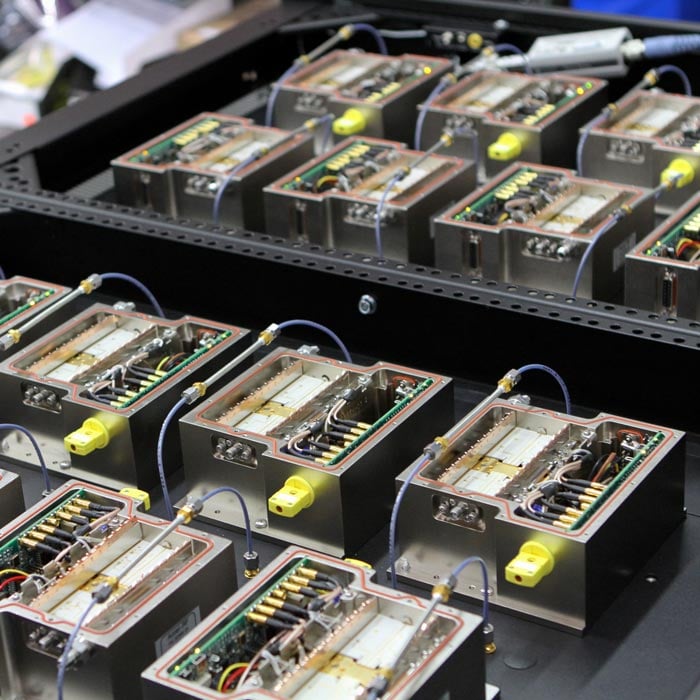
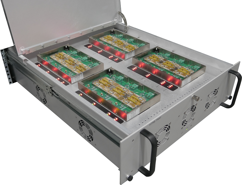
Key design features of the industry standard Accel-RF AARTS platform have been redeployed to provide a precise and economical HTRB test solution. The modular and adaptable configuration allows testing of any semiconductor technology in various package types using world-class fixturing techniques. Precision-controlled heater elements are used rather than an oven-based approach to provide finite temperature resolution and greater test flexibility. Multi-channel test drawers stack within a rack to provide maximum channel density with a minimal lab footprint.

The DC bias in this fully turnkey system is provided by power control units (PCU modules) embedded and controlled through the LifeTest software and system controller. The HTRB Tester supports the optional integration of a Semiconductor Parameter Analyzer (SPA) for automated in-situ characterization measurements.

High-Voltage Switching

The advanced development of new technologies, such as SiC and GaN, has opened the opportunity for more efficient and higher voltage/power performance in switching and power management circuits. Their high cutoff frequencies, low on-state resistance, and very high breakdown voltages can increase the power supply’s power handling densities approaching hundreds of watts/inch.

The reliability of these new technologies and techniques is critical for realizing practical applications. While Silicon devices have a rich history of proven reliability, these newer compound semiconductor technologies are too new to have a reliability history and have not been well proven.

As new device technologies mature, it is important to verify device reliability before deployment in new terrestrial and space-based systems. It is challenging to obtain standard device degradation data when operating in a powered pulsing application. The speed at which catastrophic failure occurs implies it is often impossible to assure the same failure mechanism has occurred, which is imperative for reliability calculations.

What is a Soft-Switching Test?

Reliability testing of switching power devices requires the balance of several competing challenges. The first is to understand the intrinsic reliability under application conditions without destroying the device as failures are induced. To properly analyze this, a “soft-switching” methodology is useful. This approach applies a high-voltage signal when the device is OFF, followed by a high current surge when the device is ON. In the OFF state, there is minimal current (leakage), and in the ON state, there is very little voltage (assuming RON is small); hence, power dissipation in the device is minimized in either state.

​​A competing requirement for reliability evaluation is realizing a circuit that emulates a real-life application in what is referred to as a “hard-switching” operation. In a real application, due to reactive loading, there is a small interval of time during each cycle in which high current and high voltage can exist simultaneously in the device. For example, in a 1-MHz switching regime (i.e., 500ns ON and 500ns OFF), there might be 1- to 10-ns in which high current and high voltage exist simultaneously. Depending on the duty factor of such a condition, this can significantly increase the power dissipation in a device. While this is very application dependent, it is nevertheless a reality and can dramatically affect reliability.

The Key Objectives of Soft-Switching

Soft-switching is a specific mode of operation where power devices discreetly switch from a high voltage, low current state to a low voltage, high current without any overlap. This operation, paired with elevated temperature, provides the opportunity to look for a change in the Drain Source ON Resistance, RDS-ON. As resistance increases and a change in RDS-ON is detected over the part's lifetime, that can result in performance degradation of the device. So this Soft-switching test functions as an accelerated life test to make the change in RDS-ON occur in a reasonable amount of time. This allows power device manufacturers to extrapolate the product lifetime and perform analysis for process improvement. 

Factors for Successful Testing

The concept of “soft-switching” implies avoidance of the condition in which high-voltage and high-current may exist simultaneously. As noted earlier, this can result in excessive power dissipation, which can lead to extremely fast device destruction in a time frame for which it is impossible to protect – after which failure analysis is unavailable.

Because the requirement to pulse the devices on and off very quickly is challenging, the test system needs to have precise digital controls to operate the DUT in a controlled manner. Precise biasing of the device and measurement of the RDS-ON value are also required for successful testing since that measurement needs to be captured and tracked on a microsecond scale throughout a 1000-hour test.

Accel-RF High Voltage Test Systems

The Accel-RF Power-Switching Test System can measure reliability under various conditions for switching power applications up to 1kV (off) and 25A (on) at rates up to 1-MHz switching frequency, dependent on voltage. By leveraging technology developed for the RF burn-in tray platform with new fast switching measurement techniques, this system can support the testing of multiple devices under elevated temperature stimulus in a small physical area and offers the flexibility to test both soft- and hard-switching applications. The Accel-RF Power-Switching System is the most flexible and accurate power switching platform available on the market.

The HighVoltage Soft-Switching Module handles all of the dynamic switching between the high-current and high-voltage modes, including the charging and discharging of the device capacitance. Thus, the device leakage current at high voltage and ON resistance at high current may be measured without residual thermal effects that would exist were the device to do the switching.

In the case of the hard-switching test, the challenge is simulating a large “load” condition without having to dissipate that power locally. Accel-RF has developed a technique using recirculating currents in which the device and load operate in tandem to emulate the full stress on the device under test (DUT) while only dissipating the power that would normally be residual in the application (i.e., a high-power load is not required).

As is evident in either scenario, accurate measurement of the instantaneous high-voltage and/or high-current values in the fast switching (up to 1-MHz) environment is highly desirable. Using small aperture track-and-hold techniques, the Accel-RF system can measure synchronized instantaneous ON-state resistance and OFF-state leakage values obtained at user-defined points in the switching waveform. Accel-RF systems include integration of the Keysight B 1505 SPA instrument for making the RDS-ON and current collapse measurements. This allows for easy in-situ characterization of the devices at regular intervals without having to remove the devices to perform characterization on a different test bench.

Application Testing

As the product development lifecycle moves through technology characterization and device characterization to determine intrinsic reliability and establish fabrication processes, reliability testing shifts to product qualification tests on more mature devices and products that will be sold into the marketplace. One such application test is High-Temperature Operating Life.

What is HTOL?

HTOL is a reliability testing method that accelerates the lifespan of a DUT through electrical and increased temperature stress at or near its maximum operating conditions. An accelerated aging factor (AF) multiplier allows the calculation of the expected life of the DUT based on the length of testing time, typically 1000 hours for HTOL. This test exercises each substructure of an IC's design, so testing reveals precise information about the device's lifespan and likely failure points due to stress.

Key Objectives of HTOL

Once a new product is defined, HTOL is performed on a representative sample size of devices to validate expected performance. Testing should reveal no change in performance over the testing period. The goal is not to drive the device to failure as with ALT, but the life is taken out of the part in this stage and it would not be sold into the market. HTOL also differs from burn-in, which is more concerned with screening devices for early life failure. So, HTOL testing occurs for longer periods compared to production burn-in testing. Assuming the HTOL tests are successful and no further failure analysis is required, the remaining parts can move on with the final stages of production and quality assurance testing.

Factors for Successful HTOL Testing

Thermal Management

HTOL tests typically run at the “do not exceed” temperature on the datasheet that will be published with the device, which could be around 225°C compared to 350°C and higher with accelerated life testing. Maintaining this lower baseplate temperature on many high-power devices introduces a unique set of challenges. Along with a heater control and thermal isolation, test systems will also need a cooling element to maintain that precise temperature for the duration of the test.

Multi-Channel Support

As with all types of reliability testing, significant sample size is required to produce statistically meaningful results. Therefore, the ability to analyze multiple sets of devices instead of testing one device at a time offers a distinct advantage in collecting reliability data in a shorter, more reasonable amount of time.

DC and RF Considerations

There are similar factors at play for DC and RF HTOL testing as with other accelerated life tests. While DC testing demonstrates that the semiconductor process line is fabricating devices within specific performance tolerance guidelines, it does not provide information about how well a device will perform in a specific application, especially an RF power application. RF testing validates the device’s adherence to specification levels expected by the end-user and most likely guaranteed by the manufacturer’s datasheet. 

In addition, RF performance with age is a primary metric required by the customer in reliability verification of the technology and chip design. Therefore, manufacturers working to deliver high-yield wafers for stringent RF applications must adopt levels of RF testing to increase the probability of ending up with a “known good” device for shipment to the customer.

Integrated Application Specific Testing

External requirements can play a big part in the testing program a manufacturer needs to adopt. That’s why it’s important at this stage to perform these reliability tests under the conditions and stresses the devices will encounter in the field. These results provide important data not only to the quality assurance team but also to the marketing and sales team to provide proof to the customer.

Special equipment for application-specific testing must be easily integrated into the test systems to replicate actual field conditions. For instance, standard RF, DC voltage, and heat tests will not provide the necessary data for GaN devices on the 5G network. Testing under WCDMA modulation is one method to test devices under conditions seen in the field to produce more accurate reliability data. One straightforward way to measure device linearity degradation is by tracking the change in the Peak-to-Average Ratio (PTAV) of the modulated signal delivered to the device. By testing with WCDMA modulation, the format employed by 5G standards, PTAV deterioration can help extrapolate accurate statistics on device performance under actual operating conditions.

Another example of an application-specific parameter is intermodulation distortion (IMD), which is a critical figure-of-merit (FOM) in communication system designs such as software-defined radio (SDR) and 5G New Radio (NR) digital transmitters. If IMD characteristics of the power amplifier’s semiconductor device suffer any signal linearity degradation with age and environmental effects, it will harm the overall performance of the communication system and network.

Accel-RF HTOL Test Systems

Accel-RF offers an array of multi-channel HTOL system options with an integrated software and hardware platform that provides an unparalleled ability to simultaneously test a larger number of devices over a wide array of bias settings and at elevated temperatures. Both DC and RF-HTOL test systems are available to meet all test requirements. This platform is ideal for long-duration HTOL tests, with each DUT being independently temperature-controlled. Testing at an elevated temperature, up to 200°C baseplate, is calibrated to the DUT package reference plane and is precisely controlled throughout the test duration by proprietary software and hardware embedded in the platform. The system is designed to manage the high power dissipations of mature products, such as multistage MMICs and high-power RF devices. Air and water-cooling options are available depending on DUT power dissipation.

The platform is uniquely constructed for application-specific testing. External instruments required for special testing can be easily integrated into the system, such as a signal generator capable of modulation schemes. The platform is delivered with individual, removable RFtest fixtures and interfaces with precision characterization instruments, such as a Semiconductor Parameter Analyzer (SPA).

Quality Assurance

The final stage of a product’s development and reliability journey focuses on quality assurance, also known as extrinsic reliability. Once designers select a specific application and determine suitable packaging for the device, they switch to extrinsic testing. This next stage of reliability testing determines the device’s performance characteristics in real-world applications with the goal of eliminating early field failures. 

Manufacturers use extrinsic reliability testing for quality assurance before shipping products to their customers. So while intrinsic testing pushes the device until it reaches failure mode, extrinsic testing must preserve the device for shipment to customers. In addition, extrinsic testing determines the suitability of a part for a specific application by identifying failure mechanisms resulting from operating the device as intended.

Burn-In Testing

Burn-in is a short-duration stress test that, when performed over a large sample size of identical device types, allows the manufacturer to capture a statistically based snapshot of the field performance of the device. Any atypically performing device is removed from the lot and not sent out to the customer. A burn-in test places devices under typical operating conditions in a controlled environment to cause defective products to fail before they reach the end-user.

Key Objectives of Burn-In

Semiconductor devices must perform their intended function for an expected period under all possible environments encountered in the field. Intermittent operation and poor performance are included in assessing a system’s failure rate. A high failure rate is unacceptable under any circumstance. 

Field failures can lead to costly repairs, product recalls, and customer dissatisfaction which will harm both the bottom line and the viability of a manufacturer. Thanks to burn-in, the elimination of suspect devices from the field population significantly increases the probability that devices will operate to customer expected levels of reliability. Further, an ongoing burn-in test plan is essential for statistically-based process control management of the production line.

Screening weakened devices is accomplished by putting the components under conditions designed to expose the samples to enhanced field environments to expose atypical performance parts. Burn-in seeks to uncover issues not related to the device itself but extrinsic failure effects such as the bond wiring to the device or the durability of the package mounting or soldering. 

Elevated temperature and voltages provide enhanced stressors to induce failures. By placing the components in specially designed testbeds that subject them to carefully calibrated harsh conditions, test technicians can identify the non-conforming devices while not impacting the lifetime of the other test devices.

Factors for Successful Burn-In

Thermal Isolation

Manufacturers can’t afford device malfunctions due to overheating during testing since burn-in testing is performed on application-ready devices. Your test solution must be able to thermally isolate a DUT, removing the heat from other components around the DUT so the whole fixture isn’t affected. Test temperatures are lower than in accelerated life testing, and the time spent in burn-in is much less than during an ALT test. Burn-in test temperatures usually reach 150°C or less, and test increments range from a few hours to a few days.

RF vs. DC

A consequential decision point in burn-in testing is determining whether to run DC or RF burn-in tests. This decision mirrors that of DC vs. RF tests for accelerated life testing. While DC tests are typically less expensive, time-intensive, and complex, they should only be performed on parts associated with lower-output transmitters. However, if the part is going into a high-rel application like space or satellite, for instance, an RF test is necessary to truly replicate the harsh operating conditions the devices will be subjected to.

Easy Implementation

Due to the nature of burn-in being a high volume, short duration test, the ease of implementation for the operator is critical. A fast and flexible solution that provides accurate data is the key to expediting product delivery. Efficient burn-in systems require a fixture design that allows for fast loading and unloading of devices and easy portability of that device to other environmental stress tests. 

Channel Density

Burn-in systems with multi-channel support are critical for various reasons. Maintaining a minimal system footprint is essential due to the limited space available in most production labs. High channel density allows for a greater test volume that minimizes cost and ensures the production process continues efficiently.

Software

Integrated hardware and software systems are needed to maintain precise bias and temperature levels. Properly designed systems also leverage the software component to provide automated analysis to evaluate parts for key parameter changes. The software can then return visual indicators like a green or red color to signal to the operator that parts have either passed or failed the burn-in test.

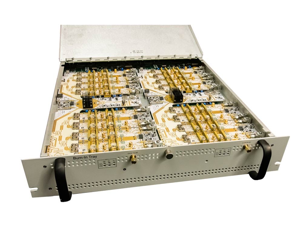
Accel-RF Burn-In Test Equipment

The modular architecture of the Accel-RF HTOL burn-in system provides the flexibility to qualify multiple device types at a low cost-per-channel and minimal lab footprint. The rack configuration has all power supply control units and PCU modules embedded and controlled through the LifeTest software and system controller. Auto-Bias features for gate/base and drain/collector levels, maximum allowable levels, and on/off sequencing are programmable in the PCU setup. Each channel or DUT is independently measured, but some stimuli are shared between channels in this platform architecture to provide an economical solution for large-scale testing. All temperature control and monitoring are done either individually or through small groups of DUT channels. Temperature setting and control is achieved through the LifeTest software with continuous update and control.

Intermittent Operating Life Test (IOL)

IOL is another type of quality test seeking to uncover extrinsic reliability issues with packaged devices. An IOL test aims to determine the integrity of the package assembly, ensuring that the chip is attached to the package securely and the bond wiring to the package is sound. Cycling the device on and off replicates the thermo-mechanical stresses experienced in typical field conditions.

Key Objectives

IOL tests are performed by activating the drain bias, allowing it to sit for 30 seconds, and quickly removing the bias. This sequence is repeated a specific number of times, often up to 5,000. Along with nominal elevated baseplate temperatures, typically 80-85°C, the generated power dissipation elevates the temperature inside the device, which can affect the interface to the device and cause excessive wear to the device if fractures occur.

Typical parameters used to monitor performance are thermal resistance, threshold voltage, ON-resistance, gate-emitter leakage current, and collector-emitter leakage current. Failure occurs when the thermal resistance or the ON-resistance increases beyond the maximum value specified on the data sheet.

Factors for Successful IOL Testing

Test Setup and Response Times

Proper test equipment selection and configuration are essential to creating an efficient IOL test that produces reliable results in a reasonable amount of time. Minimizing the cycle time ensures the testing regime doesn’t extend from days into months. Considering tests may cycle drain bias on for 30 seconds and then off for 30 seconds, the software and equipment play a large role in accurately controlling power and bias supplies to eliminate long lags in response times.

System Requirements

As with most types of reliability tests, there are common system requirements that apply to IOL testing. Maintaining precise temperature control and thermal isolation at the fixture level ensures test systems produce accurate reliability data.

Specific to IOL, the drain/collector power supplies that bias the devices are cycled on and off in a controlled manner. This type of operation requires precise timing and digital controls to gate these pulses. The voltage waveforms must also be clean pulses with minimal overshoot and ringing.

High-density, multi-channel systems allow testing a large sample size of devices to produce the required statistical data to extrapolate reliability data.

SPA Integration

Integrated semiconductor parameter analyzers are a beneficial tool to perform device characterization efficiently. SPA integration allows operators to automatically characterize the part before and after the IOL test to measure key performance indicators for change.

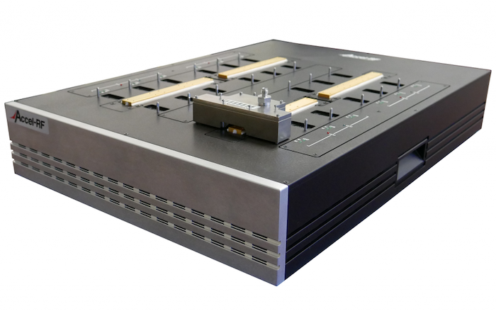
Accel-RF IOL Equipment

Accel-RF offers a multi-channel benchtop system with an integrated software and hardware platform that provides an unparalleled ability to simultaneously test a larger number of devices over a wide array of bias settings and at elevated temperatures. This platform is ideal for IOL tests, with each DUT being independently pulse-controlled for DC bias stimulus. The user programs the timing parameters of the cycle period and pulse width to meet their test requirements. Testing at an elevated temperature, up to 300°C, is calibrated to the DUT baseplate and is precisely controlled throughout the test duration by proprietary software and hardware embedded in the platform.

This 12-channel benchtop solution can be cascaded with multiple units to gradually build channel capacity to capture statistically meaningful reliability data. The system features a superior thermal design allowing for higher temperature testing up to 300°C and utilizes speed-controlled fans to maintain precise temperature control. The platform is compatible with the industry-standard RF-ready DC fixture and interfaces with precision characterization instruments, such as a Semiconductor Parameter Analyzer (SPA).

Want to save this page to reference later?

Feel free to bookmark this page so you can easily find it. We recommend downloading this guide as a PDF so you can save it to your files or share it with your team. Please fill out the form to let us know where to send the file.

Download The Types of Semiconductor Reliability and Quality Testing Guide

Download: Accel-RF's Technologies & Core Competencies

You understand the risks involved in improper reliability testing. But how do you pitch Accel-RF to your upper management?

We’ve distilled thousands of pages of documentation and sales collateral into a short eBook that explores Accel-RF’s core value propositions. Look it over with your team and bring us in to learn more.