All semiconductor devices, whether employed in high-stakes military applications or consumer products, share a common expectation, “reliable operation." Semiconductor devices must perform their intended function for an expected time period under all possible environments encountered in the field. Intermittent operation and poor performance are included in the assessment of a system’s failure rate. A high failure rate is unacceptable under any circumstance. Field failures can lead to costly repairs, product recalls, and customer dissatisfaction which will harm both the bottom line and the viability of a manufacturer.
In response to this expectation, manufacturers have developed ways to enhance the probability of delivering the highest possible reliability to the end-user. Perhaps the best approach to achieve this goal would be to perform a short but enhanced test case of the device in the actual field stress environment, essentially validating the performance signature of the field conditions.
This environmental stress “burn-in” test, when performed over a large sample size of identical device types, allows the manufacturer to capture a statistically based snapshot of the field performance of the device. Any atypical performing device is removed from the lot and not sent out to the customer. A burn-in test places devices under typical operating conditions in a controlled environment to cause defective products to fail before they reach the end-user.
The elimination of suspect devices from the field population significantly increases the probability that devices will operate to customer expected levels of reliability. Further, an ongoing burn-in test plan is essential for statistically-based process control management of the production line.
Burn-in results are the sight-glass for detecting and improving the quality and reliability assurance over the production life cycle of the device.
Eliminating Early Failures
The time-dependent failure rate of electronic components follows a pattern known as the bathtub curve. The name comes from the shape of the graph obtained when you plot the failure rate of parts against their time in operation. The resulting curve resembles a cross-section of a bathtub with sharp curves on each end and a flat bottom.
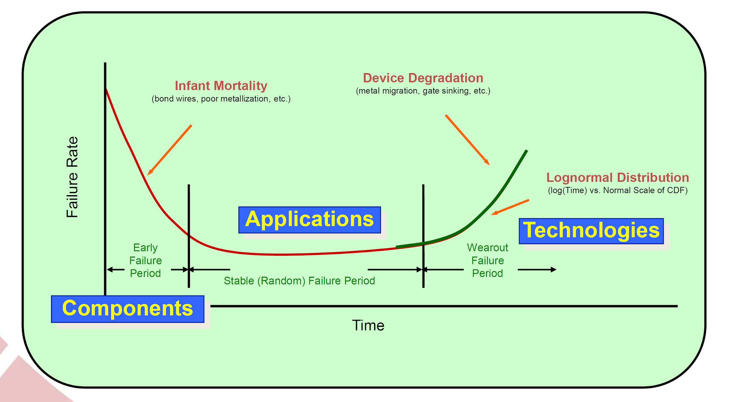
The bathtub curve is a result of the limitations of manufacturing processes and equipment capabilities implemented in the fabrication of the device. A high early failure rate results from uncontrollable anomalies that occur during the manufacturing process. As system application requirements become more advanced the requirements for device manufacturing processes are pushed to their resolution and tolerance limits. A good example comes from the requirements of new communications networks for large bandwidth channels needed for video streaming and ultra-fast data transfer.
These systems require higher frequencies of operation which drive device sizes to decrease geometries and line spacings. As fabrication processes and equipment reach their tolerance limitations, an unavoidable early failure rate increase is observed. Also, extrinsic processes not related to device fabrication itself, such as packaging and connectivity, are also common causes of early-stage failures. Over time and with feedback garnered from burn-in testing, processes and equipment parameters can be improved in key fabrication steps to reduce all areas of the failure rate bathtub curve.
The flat part of the curve represents the period of time where the failure rate is constant. This is typically referred to as the useful life of the component. This area of the bathtub curve has a failure rate for the device population that is set by the application use environmental factors, where harsh environments have a higher failure rate than a more benign environment.
The right side upward slope of the curve occurs as the combined stresses over the time of operation drive the device to the end of useful performance. Degraded performance drives an increased degradation until the end of life is realized. A statistically-based prediction of expected period of “wearout” is typically determined through Accelerated Life Testing (ALT) and should be demonstrated to occur well after the expected life requirement of the application of the end-user.
Stressing Components To Find Defects
The purpose of performing a burn-in test is to eliminate the percentage of devices that will prematurely fail before they reach expected market lifetime requirements. Screening out weakened devices is accomplished by putting the components under conditions designed to expose the samples to enhanced field environments in order to expose atypical performance parts.
Elevated temperature and voltages provide the enhanced stressors to induce the failures. By placing the components in specially designed testbeds that subject them to carefully calibrated harsh conditions, test technicians can identify the non-conforming devices while not impacting the lifetime of the other test devices.
Burn-in tests are done on deliverable products, and for that reason, the goal is not to take the life out of the product. To achieve this, test temperatures are lower than accelerated life testing, and the time spent in burn-in is much less than during an ALT test as well. Burn-in test temperatures reach 150 degrees C or less usually, and test increments range anywhere from a few hours to a few days. Contrast this with accelerated life testing, where the goal is to reach the failure point and tests run at 300 to 400 C for thousands to tens of thousands of hours.
The Importance of Thermal Isolation in Burn-In Testing
One major advantage of gallium nitride (GaN) over other technologies like gallium arsenide is in its power density. It’s the reason why GaN is the preferred solution for modern and futuristic telecommunications, automotive, and radar applications. However, with increased power density does come major challenges with temperature. Since GaN’s power density is ten times higher than other technologies, it’s also associated with 100 times the temperature regulation issues!
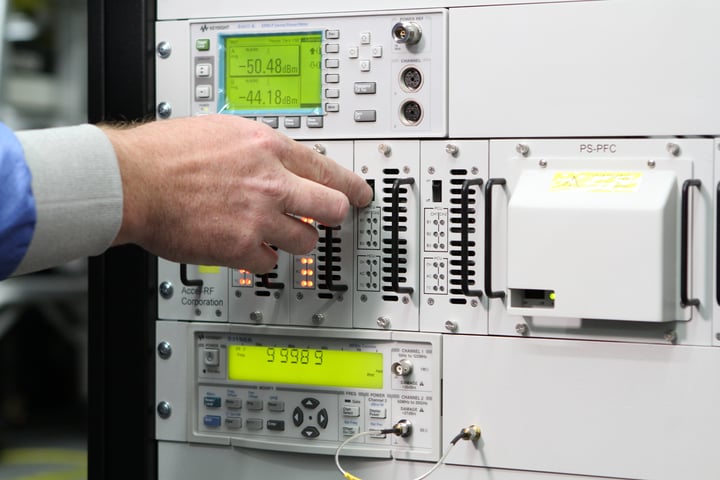
Since burn-in testing is performed on application-ready devices, manufacturers can’t afford any device malfunctions due to overheating during testing. It’s critical that your test solution be able to thermally isolate a device under test (DUT), removing the heat from other components around the DUT so the whole fixture isn’t being affected.
This is where Accel-RF’s test technology thrives. Whether accelerated life or burn-in testing, Accel-RF’s fixtures thermally isolate a DUT to control temperature with extreme accuracy. You’re not testing the system as a whole, you’re just testing the part. This allows for engineers to quickly diagnose when a part is failing over the course of normal use.
Trading Some Volume for More Reliability
Traditional destructive testing is still widely utilized for determining the failure rates during the stable period (bottom of the bathtub curve) and the wearout period (end of the bathtub curve). These tests are typically performed on standard evaluation circuits (SECs) used for monitoring different wafer lots, as opposed to deliverable products.
Properly designed burn-in testing may be used on the application-specific deliverable components in order to trigger out-of-character performance indicators without weakening properly functioning ones. Burn-in identifies and can segregate the potential early high failure rate population.
The advantage gained from this procedure is the field delivery to the customer of a statistically more reliable product population.
Incorporating Burn-In Testing
Manufacturers can perform burn-in testing in multiple variations depending on the application involved. The process of static burn-in applies higher voltage and temperature to the component, but with the device operating in atypical operating conditions. An example of this is a High-Temperature Reverse Bias (HTRB) test.
A dynamic burn-in involves running the device under more typical operating conditions that it will see in its fielded application. This can include RF bias for devices intended for wireless applications.
Typically, a combination of static and dynamic burn-in produces the best results. One of the critical benefits of burn-in is the collection of performance data. By meticulously recording the conditions and timing of each failure, a well-thought-out burn-in can help improve future testing procedures.
A consequential decision point in burn-in testing is determining whether to run DC or RF burn-in tests. This decision mirrors that of DC vs RF tests for accelerated life testing. While DC burn-in testing is often less expensive, less complex, and less stressful on the part, this testing is not an appropriate proxy to the real application intended for higher power RF devices. While DC tests are typically less expensive, time-intensive, and complex to run, they should only be performed on parts associated with lower-output transmitters. However, if the part is going into a high power transmitter like radar or on a base station, for instance, an RF test is necessary because the RF output power is going to stress that part far more than DC power will.
At the end of the day, the goal of a burn-in implementation should be increased insight and visibility into application-specific performance under stress. Each batch produced should result in more statistically meaningful data, which provides a better picture of the probability of failures in time predicted for the devices. This more confident vision of reliability can then be useful in driving fabrication process improvement to create higher quality devices or dramatically improve product yield.
Burning-In the Bottom Line
Burn-in is a valuable part of assessing semiconductor device reliability and improving fabrication process steps. While in “the old days,” field returns, after a part degraded over the course of 10+ years of normal use, provided valuable insights, markets change quickly today, and device makers no longer have ten years to learn about failure characteristics. New technologies like GaN, the evolution of 5G, radar, IoT, and more are all pushing the pace of change. When your industry is demanding instant feedback, burn-in testing provides that missing link.
Burn-in is, however, only one step in a systematic approach to ensure product reliability. True continuous process improvement to drive reliability is organizational culture. Testing will not guarantee a quality product since testing only finds problem effects. Real quality is driven by raw material quality, fabrication process control, design guideline limitation rules, and experience.
However, burn-in testing remains one of the keystones for providing statistically driven confidence to many aspects of semiconductor manufacturing. Burn-in testing enables the manufacturer historical confidence of process control, an ability to monitor and benchmark process or technology changes, and provides a pedigree certificate for convincing customers of the reliability assurance their products carry. Burn-in testing performance results may well be the “permission to play” credential for the markets of tomorrow.