Establishing reliability requirements involves probability statistics, operational lifetime expectation, and a definition of failure. Given a failure criterion, the most direct way to determine reliability is to submit a large number of samples to actual use conditions and monitor their performance against failure criteria over time. Since most semiconductor applications require device lifetimes of many years, this approach is not practical. To acquire reliability data in a reasonable amount of time, most people have used accelerated-life tests (ALT) at high temperatures. By exposing the devices to elevated temperatures, it is possible to reduce the time to failure of a component, thereby enabling data to be obtained in a shorter time than would otherwise be required. Such a technique is known as “accelerated testing” and is widely used throughout the semiconductor industry.
 For any application, the user of a part wants the assurance that the part will continue to function correctly over a given time and under certain environmental conditions. Part failure at any given time takes place when the combined effect of the stresses imposed on the part exceeds the part strength.
These statements allude to the time dependency of both part reliability and user expectation. For example, an expendable system might have a useful life of one minute while a satellite system must have a predicted life of several years. Each user has a different expectation of part reliability and a different level of commitment to pay for the assurance that the part will meet the expectation. Traditionally, the procurement of highly reliable (hi-rel) parts meant that the user of the component specified to the manufacturer additional requirements to be met in the fabrication of the part. These specifications were usually in terms of recording fabrication process steps, performing additional visual inspections, and incorporating additional screening and burn-in tests. The user of the hi-rel part was expected and usually willing to pay the cost for this increased reliability and quality assurance.
Reliability shortcomings from design to production can be minimized by incorporating, as early in the development cycle as possible, statistical process control methodologies in the fabrication of the part and by performing life test measurements. Implementing these techniques forces reliability growth to occur in conjunction with product development. For the manufacturer, this means a quicker time-to-market cycle of a reliable product that will not require costly warranty repair or replacement. For the user, it means that the state-of-the-art product can be confidently incorporated in his advanced system without the additional cost and delivery time increase associated with a traditional hi-rel part procurement.
Understanding Channel Temperature
 It is apparent that knowledge of temperature is fundamental in obtaining accurate reliability predictions from accelerated temperature testing. A semiconductor transistor will have many active elements. Some of these active elements are far hotter than other areas. The chemical and physical changes that lead to failure usually occur in these hotter regions. Therefore, one needs to know the temperature of these regions to obtain accurate determinations of activation energy, a benchmark figure-of-merit for a chemical or mechanical process change in time.
Of course, time to failure can be determined as a function of any convenient temperature, such as the base-plate temperature, however, comparison data from differing institutions are facilitated if the temperature at the failure site, such as transistor channel or transistor junction, is used. Also, active elements of semiconductor devices, such as the gate channel regions of field effect transistors (FETs), are very small. Therefore, active areas on semiconductor devices can be appreciably hotter than nearby regions of the chip, and significantly hotter than the ambient or base-plate temperature. Typically, thermal conductivity of compound semiconductor devices, such as gallium-arsenide (GaAs) and gallium-nitride (GaN) decreases with increasing temperature. This means that as the ambient or base-plate temperature increases, the temperature differences within the chip also increase non-linearly due to thermal resistance dynamic changes.
The buildup of heat in active devices is characterized by the thermal resistance of the device and the power dissipation in the device. The thermal resistance is defined as the temperature difference between the hottest spot and some reference spot, usually the ambient or base-plate temperature, divided by the power dissipated in the device. Therefore, thermal resistance is expressed in units of degrees per watt (e.g. OC/W). Note that thermal resistance will normally vary with device size and will certainly vary with the thickness of the die.
Since most RF device failures occur in the hottest area of the device, such as the FET channel, all life-test data for these devices are referenced to the channel temperature. The importance of accurately determining the channel temperature of each device submitted to life test cannot be overstressed. Variables affecting the channel temperature include ambient temperature, device thermal resistance, package and mounting materials, power dissipation, and RF signal levels. The effects of channel temperature inaccuracies can skew attempts at obtaining accurate failure rate data from ALT processes involving RF devices.
Heat generated in the transistor channel when subjected to high voltages in an RF design does not follow a proportional curve. The drain and gate bias voltages will cause excessive heating to occur even when proper sinking precautions are in place. Since RF induced failures and performance degradation are important issues for today’s wireless applications, most devices intended for signal transmitters, such as RF power amplifiers, are accelerated life tested under RF drive. Extrapolating accurate information about failures for these devices is a complicated process that requires extensive knowledge of circuit behavior at the intended frequency spectrum of the market application.
Maintaining RF Integrity at Temperatures above 200 ̊ C
When operating temperatures reach levels above 200 ̊ C in the FET channel, RF performance can diminish. Temperatures in the range of 200 ̊ C to 400 ̊ C in the FET channel are typical temperatures used in ALT procedures. Depending on the power dissipation in the FET channel and the thermal resistance of the device, baseplate temperatures may be 175 ̊C to 300 ̊C for an RF biased accelerated life test. These operating temperatures are not standard operating temperatures for the device application and at these high temperatures the lifetime of any part is greatly reduced.
While existing computer models of the device equivalent circuit help quantify performance in normal environments, a multitude of variables can render these estimates useless at ALT elevated temperatures. The ability to take accurate RF measurements at high temperatures is a specialized skill that reliability testing personnel must possess to carry out ALT programs. Data from these tests may be used to create viable failure models and eventually create design guidelines that will be permissible based on the fabrication process controls used in the manufacture of the device.
The key to achieving meaningful test data rests in the test fixture “chamber” that allows RF signals to be applied and measured at extremely high temperatures. The fixture must have a large amount of thermal isolation between the device mounting area and other components used in the RF circuit design, such as RF connectors, capacitors and resistors used for stability networks that prevent unwanted oscillations in the FET, and the RF substrate material used for the input and output RF signal.
Specifically, for RF devices intended for use in high power amplifiers, ALT must include some amount of testing with RF energy applied. This is done to present an AC voltage swing on the input terminal of the device that will be like the stimulus in the power amplifier application. Similarly, the RF signal on the input will also put the voltage swing on the output terminal in a large-signal load line condition. This condition is a severe operating application on the device and may drive failure mechanisms to accelerate or cause a failure mechanism to occur.
Complying With Complex and Varying Industry Standards
Market applications for RF devices, whether commercial, military, consumer, or space, are typically controlled and regulated by industry standards. Industry standards are usually varied by market and by region of the world. For instance, the US has space qualification and reliability standards while the European Community, through the European Space Agency, has their space qualification and reliability standards.
Additionally, commercial guidelines exist for most industries such as automotive, telecommunications, and RF sensors that vary by country and region. Typical standards and guidelines include Electrical and Electronic industry standards (JEDEC), US Space Qualification Guidelines (NASA NTSS), and ESA Space Qualification Guidelines (ECSS).
Performance degradation with age in key RF parameters will be part of the ALT test result data. Many field applications may be susceptible to RF performance degradation in key performance parameters. Degradation in performance for these parameters would cause the system to not be able to perform its intended function and render the system inoperable, a failure. This is a critical aspect for RF ALT programs. Device performance degradation are sources of system failures. System failures cause network problems and will drive cost and complexity to mitigate these failures from pulling down the network.
Results from ALT programs will be the “permission to play” credentials needed to meet qualification in any intended market application (space, commercial, industrial).
Overcoming ALT Hurdles To Realize Market Triumph
Building high-quality electronic devices requires the use of ALT to speed up the development process. If reliability tests were performed in real-time circumstances, the time-to-market for new products would be too protracted to satisfy customer and market demands.
ALT systems have the capability to achieve 300 ̊C baseplate temperatures. This allows the device under test (DUT) to achieve channel temperatures in excess of 400 ̊C which is required for accelerating failure and parametric degradation to occur within acceptable time frames, approximately three - fourth months.
ALT systems have the capability to hold the channel temperature constant with varying DC and RF parametric changes during a long duration ALT. This is very important since the location of the failure is in the channel area of the device. Without this capability the channel temperature, used as the acceleration determination parameter for calculating activation energy of the failure mechanism, would vary wildly during the test as power dissipation changes. Channel temperature varies drastically with DC and RF degradation in GaN, and other wide bandgap materials, due to their high-power density.
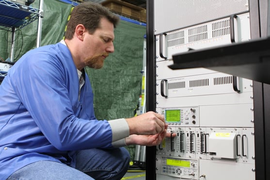 ALT systems have additional parametric instruments embedded in the unit that can be used to perform swept dynamic measurements for both DC and RF parameters. These dynamic measurements are used to extract key degradation in established device figures of merit (FOM) that benchmark industry failure requirements such as transconductance, drain-to-source resistance, and RF power output slump.
Quantitative reliability requirements provide specific design goals and criteria for assuring that the device will meet intended durability and life. Use of reliability predictions derived from ALT during the design phase of the development life cycle should be used to analyze design reliability; perform sensitivity analyses; investigate design trade-offs; verify compliance with specific industry standards; and make design and operations decisions based on reliability analysis outputs against these requirements. Data from ALT programs used in early device development form the basis for long range strategic information used to establish market viability and differentiation for a product launch. Understanding gained from reliability predictions and performance degradation against environmental and stress conditions should be used to determine not only compliance to an industry standard but to uncover avenues to best commercial practices that insure technology leadership sustainability.


