
Enabling the semiconductor revolution
webinar: gallium-nitride (gan) reliability

Watch this webinar to learn more about:
- Quality Assurance vs. Intrinsic Reliability
- Failure-Rate Bathtub Curve
- Technology Development Curve
- GaN Reliability Test Concepts
- GaN vs. SiC & SJFETs
- Hard vs. Soft Switching
- Overview of Attributes Comparison Chart
- Techniques to Mitigate Current Collapse
- Measurement Challenges of GaN
This webinar provides an in-depth look at everything you need to know regarding GaN reliability. From comparison analysis to understanding failure rates to customized "How-Tos," this webinar covers it all.
What you'll learn in this webinar: here's a sneak peek
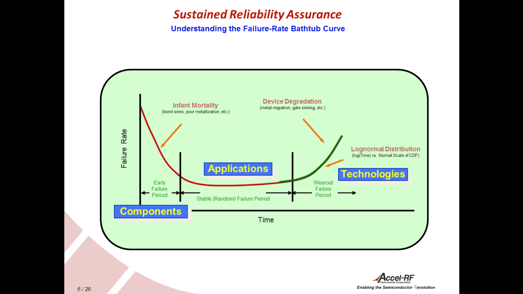
1. Understanding the Failure-Rate Bathtub Curve
The bathtub curve is a result of the limitations of manufacturing processes and equipment capabilities implemented in the fabrication of the device. A high early failure rate results from uncontrollable anomalies that occur during the manufacturing process.
As system application requirements become more advanced the requirements for device manufacturing processes are pushed to their resolution and tolerance limits. It's important to understand the failure-rate bathtub curve so you can reduce the likely hood of failure "time bombs" happening in the field resulting from unknown defects or weaknesses.
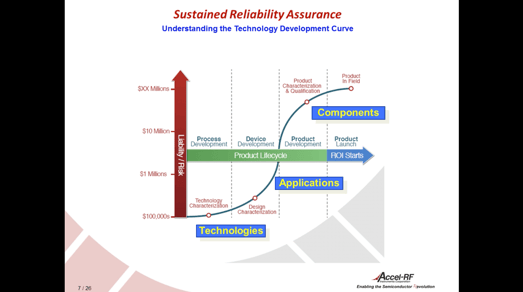
2. Understanding the Technology Development Curve
You can also apply the concept of sustained reliability assurance to understanding the technology development curve.
Understanding the technology development curve will help you identify what drives the application and how this application will effect the failure rate. This curve will also help in determining liability risks through the product lifecycle.

3. Understanding the Figure of Merit (FOM) Comparison
Use this graph to better understand the that the FOM of GaN HEMTs is much lower than the SJ and SiC MOSFETs.
This plot will help explain that the GaN HEMTs are capable of switching at much higher frequencies, enabling smaller and lighter power supplies.